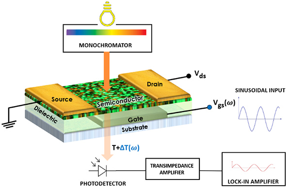
Investigating the charge transport mechanisms in solution-processed semiconductors is fundamental towards the optimization of organic electronic devices. The charge transport phenomena such as thermally activated hopping or band like regimes depends not only on the specific chemical structure of the organic semiconductor, but also on the processing conditions that dictates the degree of structural order in the casted films.
In our group, we investigate solution-processed semiconducting polymers, small-molecules and carbon nanotubes in a field-effect transistors (FET) device. The semiconductor forms the active channel of the FET where the fundamental charge transport parameters such as charge carrier mobility or threshold voltage can be extracted.
One of the techniques employed to study such phenomena is charge modulation spectroscopy (CMS). This technique allows to directly probe the spectral features induced by a periodic modulation of the charge density in the FET channel. CMS detects small variations of the film absorbance and it is sensitive to the accumulation of free charges only. This permits to correlate the molecular and crystalline structure of the semiconducting film with charge relaxation and charge transport in the device’s working conditions.
Coupling the CMS setup with a confocal microscope, we can also perform charge modulation microscopy (CMM), which allows to obtain local CMS signal with micrometric resolution. This is a power tool enabling to monitor how charges are distributed when injected in the channel and to draw a correlation with structural order of domains present in the semiconducting film.

![Mapping Orientational Order of Charge-Probed Domains in a Semiconducting Polymer [Reprinted with permission from { ACS Nano 2014, 8, 6, 5968–5978}. Copyright {2014} American Chemical Society]](/documents/211942/301707/CHARGE-TRANSPORT2-rev.jpg/bc0ee162-e44a-2787-4faa-48aedd415d59?t=1617270348265)